- 您现在的位置:买卖IC网 > Sheet目录3828 > ATMEGA169P-16MCU (Atmel)MCU AVR 16K ISP FLSH 16MHZ 64QFN
PIC16F946
DS41265A-page 196
Preliminary
2005 Microchip Technology Inc.
16.3.4
TIME-OUT SEQUENCE
On power-up, the time-out sequence is as follows: first,
PWRT time-out is invoked after POR has expired, then
OST is activated after the PWRT time-out has expired.
The total time-out will vary based on oscillator configu-
ration and PWRTE bit status. For example, in EC mode
with PWRTE bit erased (PWRT disabled), there will be
no time-out at all. Figure 16-4, Figure 16-5 and Figure
16-6 depict time-out sequences. The device can exe-
cute code from the INTOSC while OST is active, by
enabling Two-Speed Start-up or Fail-Safe Monitor (see
Since the time-outs occur from the POR pulse, if MCLR
is kept low long enough, the time-outs will expire. Then,
bringing MCLR high will begin execution immediately
(see Figure 16-5). This is useful for testing purposes or
to synchronize more than one PIC16F946 device
operating in parallel.
Table 16-5 shows the Reset conditions for some
special registers, while Table 16-5 shows the Reset
conditions for all the registers.
16.3.5
POWER CONTROL (PCON)
REGISTER
The Power Control (PCON) register (address 8Eh) has
two Status bits to indicate what type of Reset that last
occurred.
Bit 0 is BOR (Brown-out Reset). BOR is unknown on
Power-on Reset. It must then be set by the user and
checked on subsequent Resets to see if BOR = 0,
indicating that a Brown-out has occurred. The BOR
Status bit is a “don’t care” and is not necessarily
predictable
if
the
brown-out
circuit
is
disabled
(BOREN<1:0> = 00 in the Configuration Word register).
Bit 1 is POR (Power-on Reset). It is a ‘0’ on Power-on
Reset and unaffected otherwise. The user must write a
‘1’ to this bit following a Power-on Reset. On a
subsequent Reset, if POR is ‘0’, it will indicate that a
Power-on Reset has occurred (i.e., VDD may have
gone too low).
For more information, see Section 16.3.3 “Brown-Out
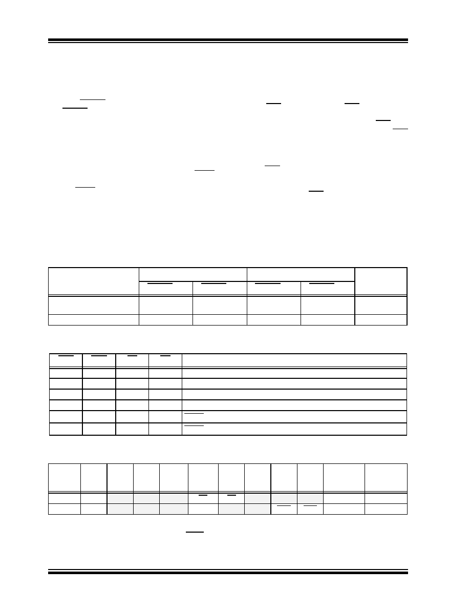
TABLE 16-1:
TIME-OUT IN VARIOUS SITUATIONS
TABLE 16-2:
PCON BITS AND THEIR SIGNIFICANCE
TABLE 16-3:
SUMMARY OF REGISTERS ASSOCIATED WITH BROWN-OUT
Oscillator Configuration
Power-up
Brown-out Reset
Wake-up from
Sleep
PWRTE = 0
PWRTE = 1
PWRTE = 0
PWRTE = 1
XT, HS, LP(1)
TPWRT + 1024
TOSC
1024 TOSC
TPWRT + 1024
TOSC
1024 TOSC
RC, EC, INTOSC
TPWRT
—TPWRT
——
Note 1:
LP mode with T1OSC disabled.
POR
BOR
TO
PD
Condition
0u11
Power-on Reset
1011
Brown-out Reset
uu0u
WDT Reset
uu00
WDT Wake-up
uuuu
MCLR Reset during normal operation
uu10
MCLR Reset during Sleep
Legend: u = unchanged, x = unknown
Address
Name
Bit 7
Bit 6
Bit 5
Bit 4
Bit 3
Bit 2
Bit 1
Bit 0
Value on
POR, BOR
Value on
all other
Resets(1)
03h
STATUS
IRP
RP1
RPO
TO
PD
Z
DC
C
0001 1xxx
000q quuu
8Eh
PCON
—
SBOREN
—
—POR
BOR
--01 --qq
--0u --uu
Legend:
u
= unchanged, x = unknown, – = unimplemented bit, reads as ‘0’, q = value depends on condition. Shaded cells are
not used by BOR.
Note
1:
Other (non Power-up) Resets include MCLR Reset and Watchdog Timer Reset during normal operation.
发布紧急采购,3分钟左右您将得到回复。
相关PDF资料
AT91SAM7XC256-CU
MCU ARM 256K HS FLASH 100-TFBGA
PIC16LF874A-I/P
IC MCU FLASH 4KX14 EE A/D 40DIP
PIC16F84-10/SO
IC MCU FLASH 1KX14 EE 18SOIC
AT91SAM7XC128-CU
MCU ARM 128K HS FLASH 100-TFBGA
PIC18F2458-I/SO
IC PIC MCU FLASH 12KX16 28SOIC
PIC18F4455-I/P
IC PIC MCU FLASH 12KX16 40DIP
AT91SAM7X256-CU
MCU ARM 256K HS FLASH 100-TFBGA
PIC16C73B-20/SS
IC MCU OTP 4KX14 A/D PWM 28SSOP
相关代理商/技术参数
ATMEGA169P-16MU
功能描述:8位微控制器 -MCU AVR 16K FLASH 512B EE 1K SRAM LCD ADC RoHS:否 制造商:Silicon Labs 核心:8051 处理器系列:C8051F39x 数据总线宽度:8 bit 最大时钟频率:50 MHz 程序存储器大小:16 KB 数据 RAM 大小:1 KB 片上 ADC:Yes 工作电源电压:1.8 V to 3.6 V 工作温度范围:- 40 C to + 105 C 封装 / 箱体:QFN-20 安装风格:SMD/SMT
ATMEGA169P-16MU SL383
制造商:Atmel Corporation 功能描述:MCU 8BIT ATMEGA RISC 16KB FLASH 3.3V/5V 64PIN MLF - Tape and Reel
ATMEGA169P-16MUR
功能描述:8位微控制器 -MCU AVR LCD 16KB FLSH EE 512B 1KB SRAM-16MHZ RoHS:否 制造商:Silicon Labs 核心:8051 处理器系列:C8051F39x 数据总线宽度:8 bit 最大时钟频率:50 MHz 程序存储器大小:16 KB 数据 RAM 大小:1 KB 片上 ADC:Yes 工作电源电压:1.8 V to 3.6 V 工作温度范围:- 40 C to + 105 C 封装 / 箱体:QFN-20 安装风格:SMD/SMT
ATMEGA169P-8AU
制造商:ATMEL 制造商全称:ATMEL Corporation 功能描述:Microcontroller with 16K Bytes In-System Programmable Flash
ATMEGA169P-8MU
制造商:ATMEL 制造商全称:ATMEL Corporation 功能描述:Microcontroller with 16K Bytes In-System Programmable Flash
ATMEGA169PA
制造商:ATMEL 制造商全称:ATMEL Corporation 功能描述:8-bit Microcontroller with 16K Bytes In-System Programmable Flash
ATMEGA169PA_1
制造商:ATMEL 制造商全称:ATMEL Corporation 功能描述:High Endurance Non-volatile Memory segments
ATMEGA169PA-AN
功能描述:8位微控制器 -MCU AVR XMEGA 384KB 105C 4KB EE32K SRAM-16MHz RoHS:否 制造商:Silicon Labs 核心:8051 处理器系列:C8051F39x 数据总线宽度:8 bit 最大时钟频率:50 MHz 程序存储器大小:16 KB 数据 RAM 大小:1 KB 片上 ADC:Yes 工作电源电压:1.8 V to 3.6 V 工作温度范围:- 40 C to + 105 C 封装 / 箱体:QFN-20 安装风格:SMD/SMT